
Wafer Sensors.
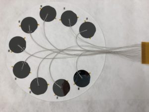
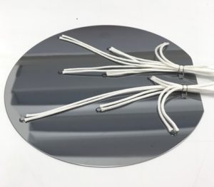
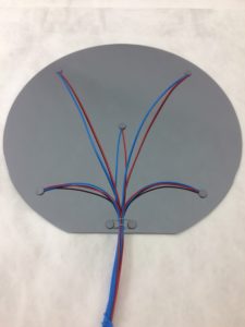
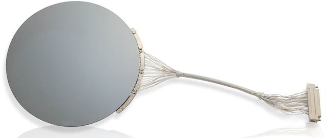
Instrumented wafers — thermocouple, bonded and RTD — for semiconductor processing equipment, where knowing and controlling the temperature at the surface of a wafer is critical.
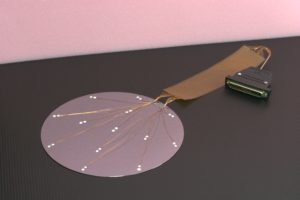
Measured at the Surface
Where the most vital processes happen
Most manufacturers embed their sensors within the wafer's core. Thermo Electric focuses measurement at the wafer's surface, where the most vital processes occur — delivering faster, more accurate response through precise placement of the sensing elements.
We have the expertise to design and install our sensors on a wide range of substrates — supplied bare, coated or patterned — with custom shapes and sizes available.

TEDAQ
Capture, map and analyze wafer temperature data
Thermo Electric's data-acquisition (TEDAQ) and temperature-mapping software provide fully integrated, multipoint temperature measurement across any instrumented-wafer assembly — an embedded hardware-and-software solution easily adapted to any wafer size.
The Wafer Range
From low-temperature RTDs to 1,200 °C laser-welded wafers
TC-350
Surface-focused thermocouple wafer for accurate, fast response. Available High-Performance (smallest sensing elements, low thermal mass) and Heavy-Duty (rugged, extended lifespan) builds.
TC-700
Higher-temperature thermocouple wafer with the same precise surface placement. Offered in High-Performance and Heavy-Duty builds for demanding process environments.
TC-1200
Laser-welded silicon with no bonding agent — one of the cleanest designs available, eliminating out-gassing for extreme high-temperature, high-purity operation.
BTC700H — Bonded Wafer
Low-profile mated wafer pair for wafer-bonding equipment — MEMS, MOEMS, silicon-on-insulator (SOI), wafer-level packaging and 3D chip stacking.
RTD Wafer
Higher accuracy and stability than thermocouple wafers, with the repeatability to maintain initial accuracy over extended periods for fabrication-equipment monitoring.

Profile & Spike TCs
Precious-metal (Type B, S, R) spike and profile thermocouples for diffusion furnaces and doping — built to be trusted by the most rigorous semiconductor processes.
Built to your wafer, your process.
Fill out our tailored quote form with your specific requirements, or reach out for more information about our instrumented-wafer solutions.
Documentation
Brochures, specifications and configuration tables